PAGE
STANDARD
NAME
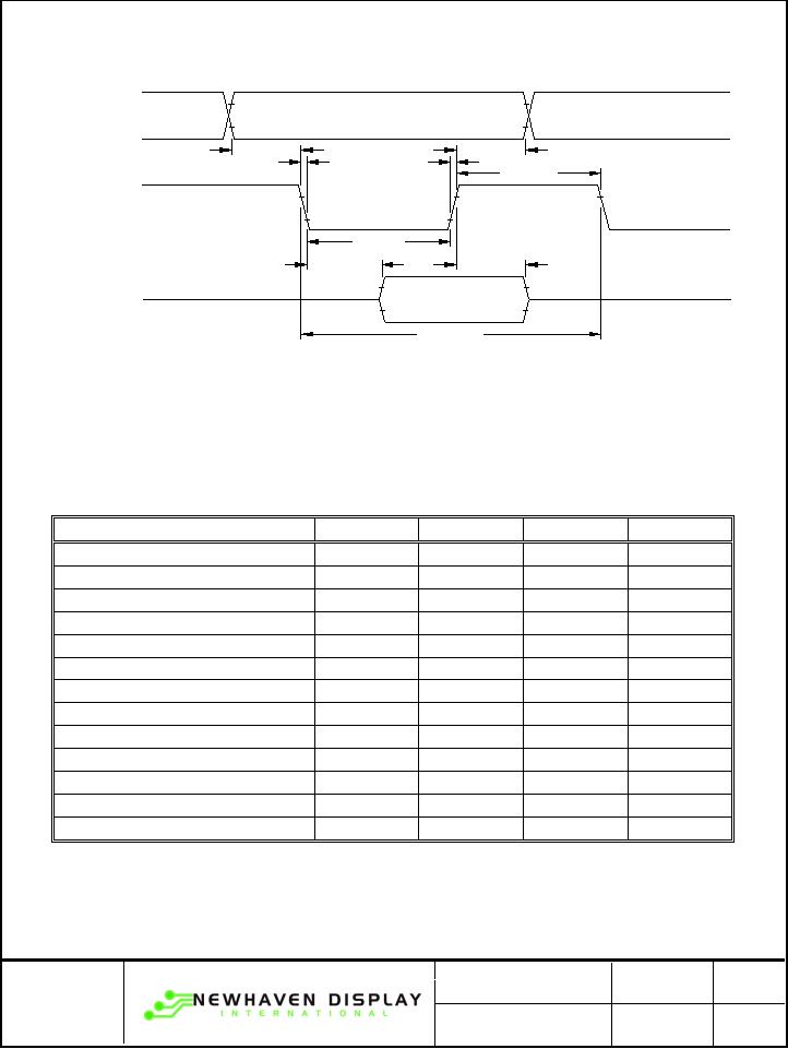
RS
RD/
DB0-DB7
tRSS
tf
tRSH
tr
tRDL
tRDH
tDHRi
tCYCRD
tDDi
Figure 6.
Intel I80-Type Parallel Interface Read Cycle Timing
3.7.4 SYNCHRONOUS SERIAL INTERFACE TIMING
(See Figures 7, 8 and 12)
Item
Symbol
Min.
Max.
Unit
STB setup time
tSTBS
100
-
ns
STB hold time
tSTBH
500
-
ns
Input signal fall time
tf
-
15
ns
Input signal rise time
tr
-
15
ns
STB pulse width high
tWSTB
500
-
ns
SCK pulse width high
tSCKH
200
-
ns
SCK pulse width low
tSCKL
200
-
ns
SI data setup time
tDSs
100
-
ns
SI data hold time
tDHs
100
-
ns
SCK cycle time
tCYCSCK
500
-
ns
SCK wait time between bytes
tWAIT
1
-
us
SO data delay time
tDDs
-
150
ns
SO data hold time
tDHRs
5
-
ns
Note: All timing is specified using 20% and 80% of VCC
as the reference points.
10/24
REV. NO.
03
DOCUMENT NO.
发布紧急采购,3分钟左右您将得到回复。
相关PDF资料
M0216SD-162SDAR8
MODULE VF CHAR 2X16 5.34MM
M0220MD-202LDAR2
MODULE VF CHAR 2X20 10.5MM
M0220MD-202MDAR1-1
MODULE VF CHAR 2X20 8.95MM
M0220MD-202MDAR1-3
MODULE VF CHAR 2X20 8.95MM
M0220SD-202SDAR1-1G
MODULE VF CHAR 2X20 5.34MM
M0220SD-202SDAR1-S
MODULE VF CHAR 2X20 5.34MM
M0220SD-202SDAR1
MODULE VF CHAR 2X20 5.34MM
M0224SD-242MDBR1-1
MODULE VF CHAR 2X24 5.34MM
相关代理商/技术参数
M0216SD-162SDAR8
功能描述:真空荧光显示器 - VFD 2 x 16 84.0 x 44.0 x 16.6 RoHS:否 制造商:Noritake 产品:Graphic Display Modules 字符计数 x 行: 模块大小 - 宽x高x厚:230 mm x 78 mm x 15 mm 观察区域 - 宽x高:166.25 mm x 41.45 mm 接口: 电压额定值:5 V 工作温度范围:- 40 C to + 85 C 封装:
M02170G-12
制造商:Mindspeed Technologies Inc 功能描述:10 GBPS LASER DRIVER - Bulk
M02171G-12
制造商:Mindspeed Technologies Inc 功能描述:M02171G-12 10GBPS LD W/DDMI ROHS-IC - Bulk
M02172G-12
制造商:Mindspeed Technologies Inc 功能描述:M02172G-12 10GBPS LD W/DDMI ROHS-IC - Bulk
M0220MD-202LDAR2
功能描述:真空荧光显示器 - VFD DIM=193.0x64.0x25.0 5 x 7 Dot RoHS:否 制造商:Noritake 产品:Graphic Display Modules 字符计数 x 行: 模块大小 - 宽x高x厚:230 mm x 78 mm x 15 mm 观察区域 - 宽x高:166.25 mm x 41.45 mm 接口: 电压额定值:5 V 工作温度范围:- 40 C to + 85 C 封装:
M0220MD-202MDAR1-1
功能描述:真空荧光显示器 - VFD DIM=146.0x43.0x19.2 5 x 8 Dot RoHS:否 制造商:Noritake 产品:Graphic Display Modules 字符计数 x 行: 模块大小 - 宽x高x厚:230 mm x 78 mm x 15 mm 观察区域 - 宽x高:166.25 mm x 41.45 mm 接口: 电压额定值:5 V 工作温度范围:- 40 C to + 85 C 封装:
M0220MD-202MDAR1-3
功能描述:真空荧光显示器 - VFD 2 x 20 146.0 x 43.0 x 19.2 RoHS:否 制造商:Noritake 产品:Graphic Display Modules 字符计数 x 行: 模块大小 - 宽x高x厚:230 mm x 78 mm x 15 mm 观察区域 - 宽x高:166.25 mm x 41.45 mm 接口: 电压额定值:5 V 工作温度范围:- 40 C to + 85 C 封装:
M0220SD-202SDAR1
功能描述:真空荧光显示器 - VFD 2 x 20 116.0 x 37.0 x 17.5 RoHS:否 制造商:Noritake 产品:Graphic Display Modules 字符计数 x 行: 模块大小 - 宽x高x厚:230 mm x 78 mm x 15 mm 观察区域 - 宽x高:166.25 mm x 41.45 mm 接口: 电压额定值:5 V 工作温度范围:- 40 C to + 85 C 封装:
